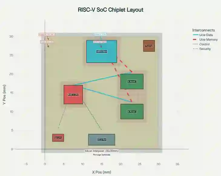
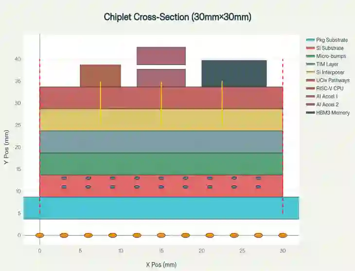
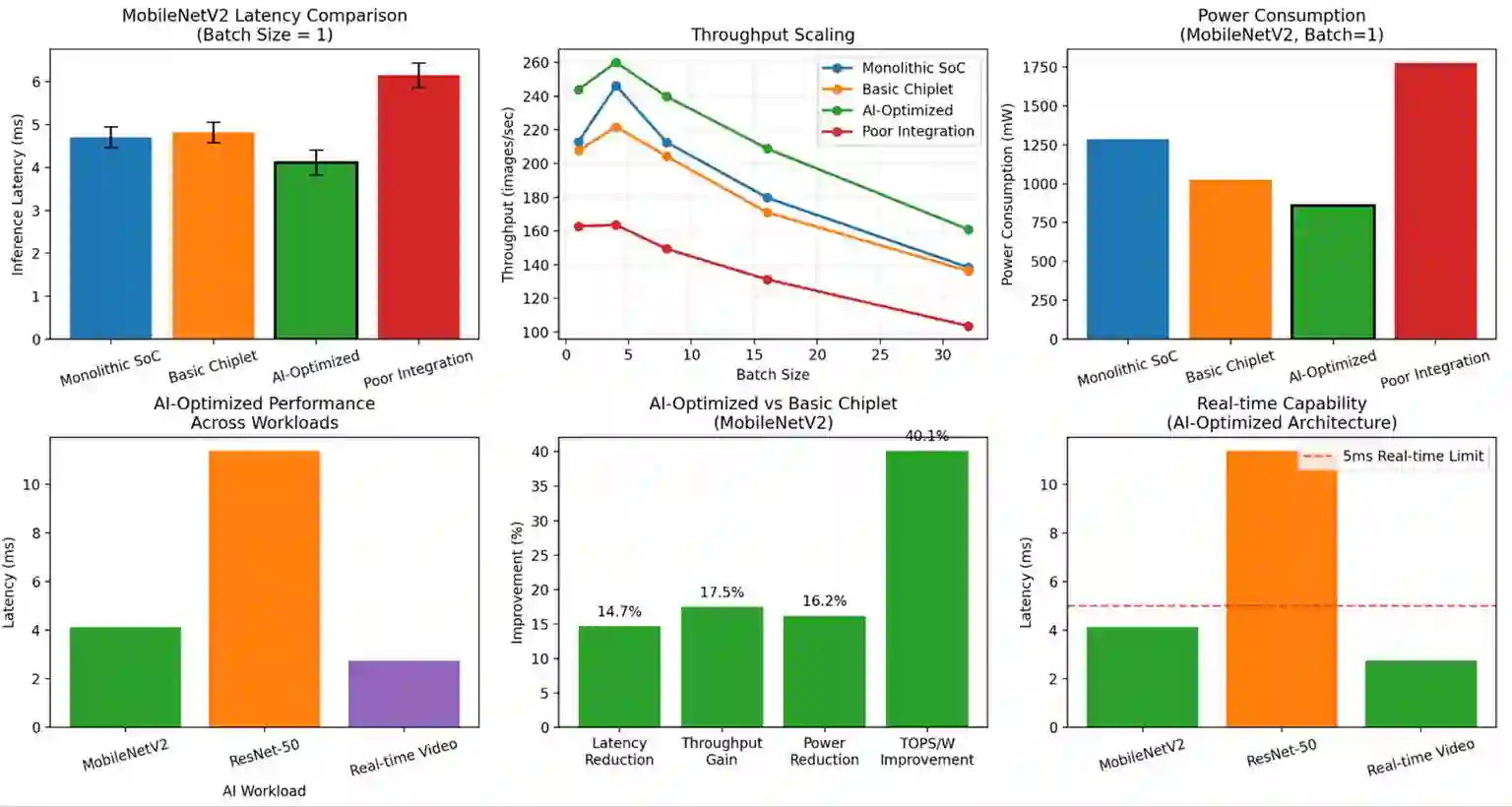
Achieving high performance, energy efficiency, and cost-effectiveness while maintaining architectural flexibility is a critical challenge in the development and deployment of edge AI devices. Monolithic SoC designs struggle with this complex balance mainly due to low manufacturing yields (below 16%) at advanced 360 mm^2 process nodes. This paper presents a novel chiplet-based RISC-V SoC architecture that addresses these limitations through modular AI acceleration and intelligent system level optimization. Our proposed design integrates 4 different key innovations in a 30mm x 30mm silicon interposer: adaptive cross-chiplet Dynamic Voltage and Frequency Scaling (DVFS); AI-aware Universal Chiplet Interconnect Express (UCIe) protocol extensions featuring streaming flow control units and compression-aware transfers; distributed cryptographic security across heterogeneous chiplets; and intelligent sensor-driven load migration. The proposed architecture integrates a 7nm RISC-V CPU chiplet with dual 5nm AI accelerators (15 TOPS INT8 each), 16GB HBM3 memory stacks, and dedicated power management controllers. Experimental results across industry standard benchmarks like MobileNetV2, ResNet-50 and real-time video processing demonstrate significant performance improvements. The AI-optimized configuration achieves ~14.7% latency reduction, 17.3% throughput improvement, and 16.2% power reduction compared to previous basic chiplet implementations. These improvements collectively translate to a 40.1% efficiency gain corresponding to ~3.5 mJ per MobileNetV2 inference (860 mW/244 images/s), while maintaining sub-5ms real-time capability across all experimented workloads. These performance upgrades demonstrate that modular chiplet designs can achieve near-monolithic computational density while enabling cost efficiency, scalability and upgradeability, crucial for next-generation edge AI device applications.
翻译:在边缘AI设备的开发与部署中,如何在保持架构灵活性的同时实现高性能、高能效与成本效益,是一个关键挑战。传统的单片SoC设计难以实现这种复杂平衡,主要原因是先进360 mm²工艺节点的制造良率较低(低于16%)。本文提出一种新颖的基于Chiplet的RISC-V SoC架构,通过模块化AI加速与智能系统级优化来解决这些限制。我们提出的设计在30mm x 30mm硅中介层中集成了四项关键创新:自适应跨Chiplet动态电压频率调节(DVFS);具备流控单元与压缩感知传输特性的AI感知型通用Chiplet互连扩展协议(UCIe);跨异构Chiplet的分布式加密安全机制;以及智能传感器驱动的负载迁移。该架构集成了7nm RISC-V CPU Chiplet、双5nm AI加速器(每个提供15 TOPS INT8算力)、16GB HBM3内存堆栈及专用电源管理控制器。在MobileNetV2、ResNet-50等工业标准基准测试及实时视频处理中的实验结果表明,系统性能获得显著提升。相较于先前的基础Chiplet方案,AI优化配置实现了约14.7%的延迟降低、17.3%的吞吐量提升及16.2%的功耗下降。这些改进共同转化为40.1%的能效增益,相当于每次MobileNetV2推理消耗约3.5 mJ能量(860 mW/244 images/s),同时在所有实验负载中保持低于5ms的实时处理能力。这些性能提升表明,模块化Chiplet设计能够实现接近单片集成的计算密度,同时具备成本效益、可扩展性与可升级性,这对于下一代边缘AI设备应用至关重要。