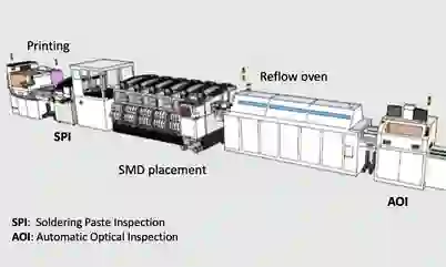
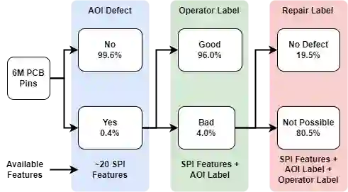
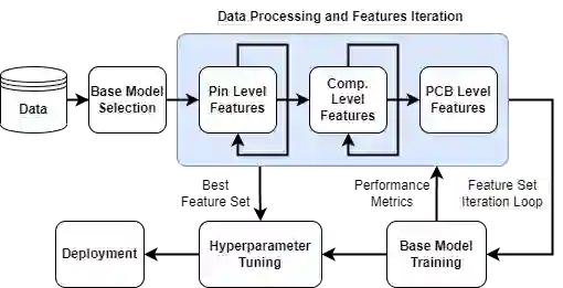
Automated detection of defects in Printed Circuit Board (PCB) manufacturing using Solder Paste Inspection (SPI) and Automated Optical Inspection (AOI) machines can help improve operational efficiency and significantly reduce the need for manual intervention. In this paper, using SPI-extracted features of 6 million pins, we demonstrate a data-centric approach to train Machine Learning (ML) models to detect PCB defects at three stages of PCB manufacturing. The 6 million PCB pins correspond to 2 million components that belong to 15,387 PCBs. Using a base extreme gradient boosting (XGBoost) ML model, we iterate on the data pre-processing step to improve detection performance. Combining pin-level SPI features using component and PCB IDs, we developed training instances also at the component and PCB level. This allows the ML model to capture any inter-pin, inter-component, or spatial effects that may not be apparent at the pin level. Models are trained at the pin, component, and PCB levels, and the detection results from the different models are combined to identify defective components.
翻译:自动检测印刷电路板(PCB)制造中的缺陷,利用焊膏检测(SPI)和自动光学检测(AOI)机器,有助于提高运营效率并显著减少人工干预的需求。本文利用SPI提取的600万引脚特征,展示了一种数据驱动的方法来训练机器学习(ML)模型,以在PCB制造的三个阶段检测缺陷。这600万个PCB引脚对应于属于15,387块PCB的200万个元件。使用基础的极端梯度提升(XGBoost)ML模型,我们迭代数据预处理步骤以改进检测性能。通过结合元件和PCB ID对引脚级SPI特征进行组合,我们还在元件和PCB级别构建了训练实例。这使得ML模型能够捕捉引脚级可能不明显的引脚间、元件间或空间效应。模型在引脚、元件和PCB级别进行训练,并将不同模型的检测结果相结合,以识别有缺陷的元件。