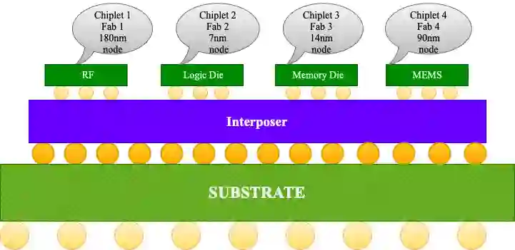
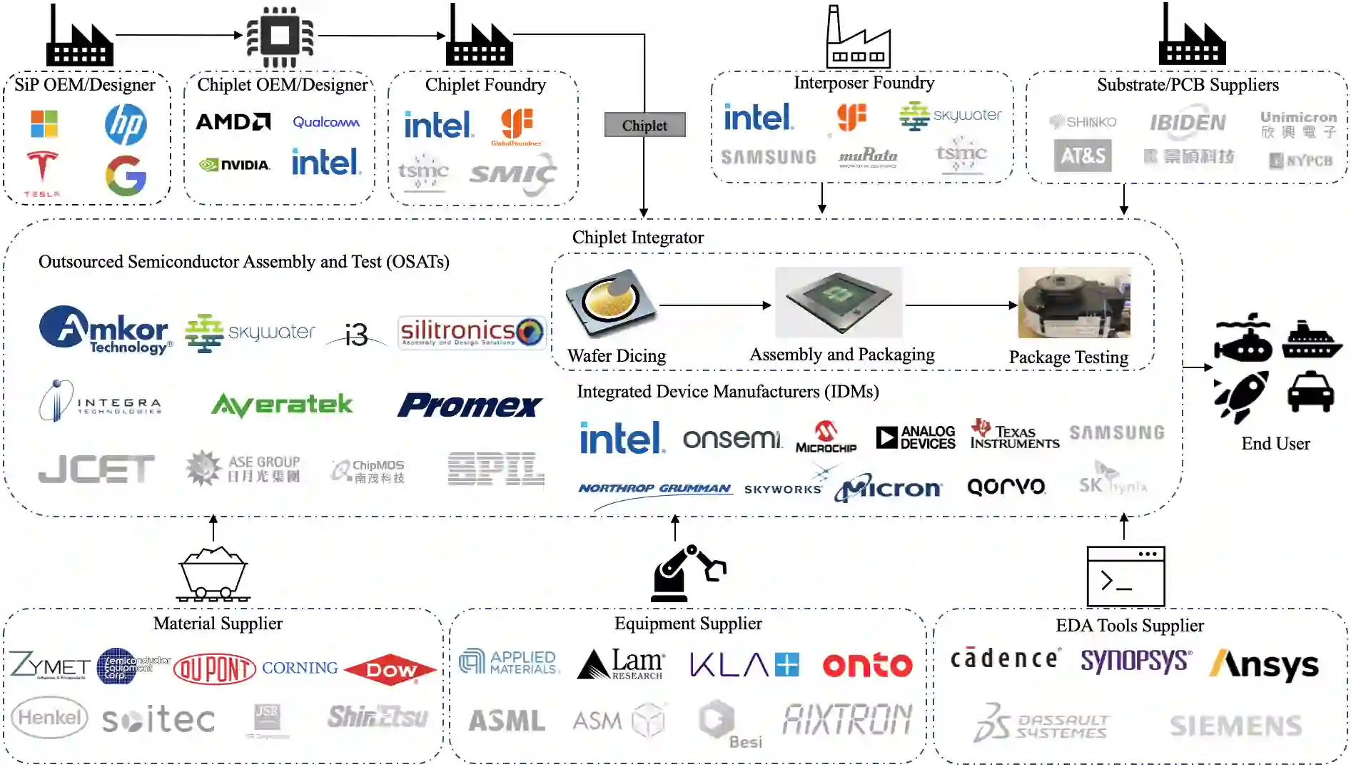
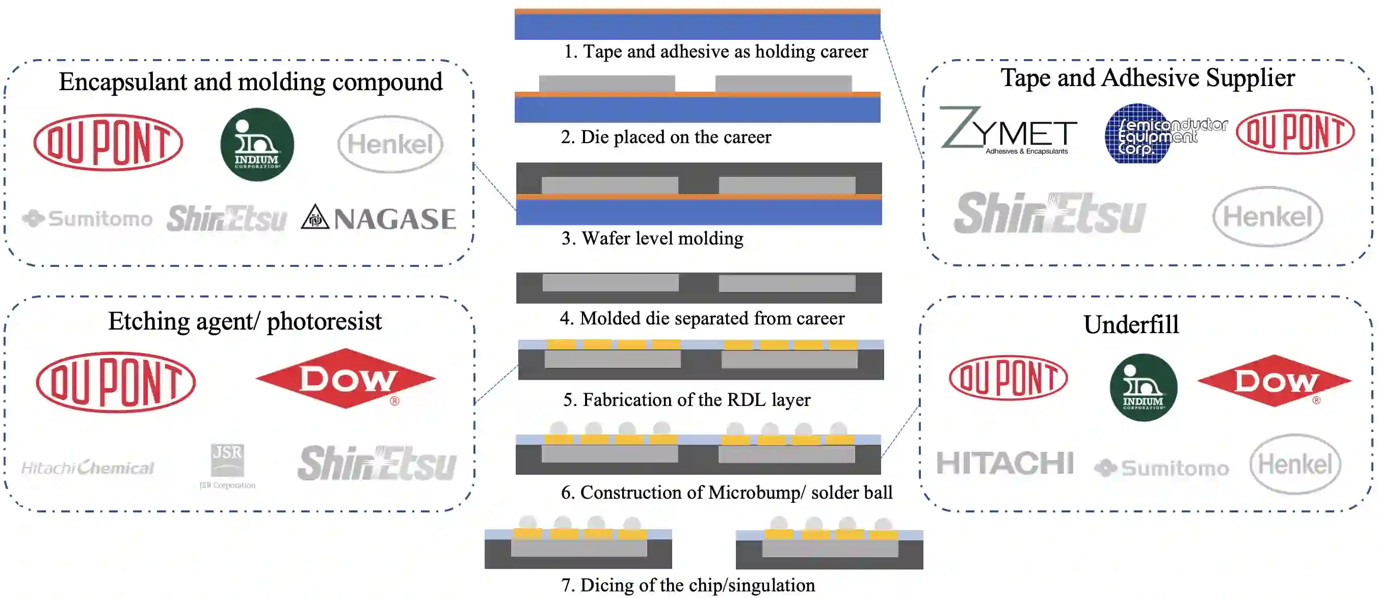
The semiconductor industry is experiencing a significant shift from traditional methods of shrinking devices and reducing costs. Chip designers actively seek new technological solutions to enhance cost-effectiveness while incorporating more features into the silicon footprint. One promising approach is Heterogeneous Integration (HI), which involves advanced packaging techniques to integrate independently designed and manufactured components using the most suitable process technology. However, adopting HI introduces design and security challenges. To enable HI, research and development of advanced packaging is crucial. The existing research raises the possible security threats in the advanced packaging supply chain, as most of the Outsourced Semiconductor Assembly and Test (OSAT) facilities/vendors are offshore. To deal with the increasing demand for semiconductors and to ensure a secure semiconductor supply chain, there are sizable efforts from the United States (US) government to bring semiconductor fabrication facilities onshore. However, the US-based advanced packaging capabilities must also be ramped up to fully realize the vision of establishing a secure, efficient, resilient semiconductor supply chain. Our effort was motivated to identify the possible bottlenecks and weak links in the advanced packaging supply chain based in the US.
翻译:半导体行业正经历从传统芯片尺寸微缩与成本降低方法的重大转变。芯片设计者积极寻求新技术方案以提升成本效益,同时在硅基芯片中集成更多功能。异构集成(HI)是一种可行方案,通过先进封装技术将采用最适配工艺技术独立设计与制造的组件进行集成。然而,采用异构集成会带来设计与安全方面的挑战。要实现异构集成,先进封装技术的研发至关重要。现有研究指出先进封装供应链中存在的潜在安全威胁,因为大多数外包半导体封装与测试(OSAT)设施/供应商位于海外。为应对日益增长的半导体需求并确保供应链安全,美国政府正大力推进半导体制造设施回流本土。但若要实现建立安全、高效、有韧性的半导体供应链这一愿景,美国本土的先进封装能力也亟待提升。本研究旨在识别基于美国的先进封装供应链中可能存在的瓶颈与薄弱环节。